60 Second Timer
1. Project Overview
|
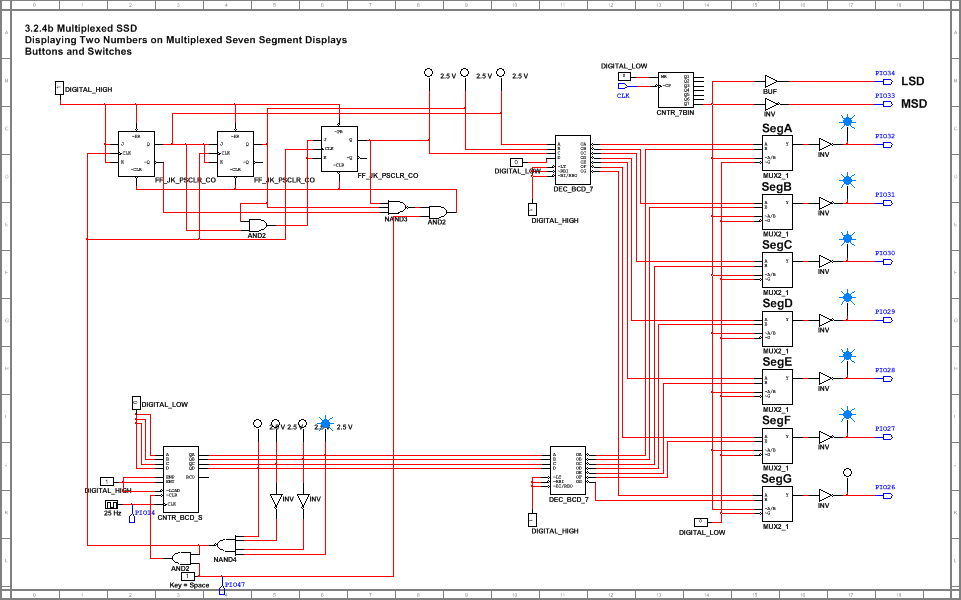
The purpose of this project is to design a sixty second timer in PLD mode then build the circuit on a breadboard. The counter should count from 00 to 59 and then back to 00 and then loop again and again. The tens place of the timer is controlled by a set of asynchronous counters designed with 3 SSI J/K flip flops. The ones place is controlled by a synchronous counter designed with a 74LS163 MSI counter. Both of the displays are using a 74LS48 BCD-to-Seven-Segment display driver. This is found in design mode.
|
|
2. PLD Circuit
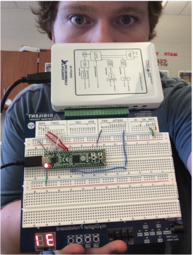
This circuit was designed in PLD Mode in MultiSim and transferred onto a PLTW breadboard using the C-Mod6 chip and the myDAQ power supply. (Cont. In conclusion)
3. Final Project Conclusions
As a whole, my circuit used both synchronous and asynchronous counters, however the counters have many differences. The synchronous counters are clocked synchronously, or simultaneously, which requires more logic than the asynchronous counters. Since they are clocked simultaneously the synchronous counters are faster. Also, the synchronous counters don't experience the ripple effect where the circuit experiences a delay and causes overlap in the display. The differences between the '163 and the '193 is quite simple. The '163 is the only gate that will show the binary number entered. The '193 can count up and down while the '163 only goes up.
When the circuit is powered and the clock is started, the '163 counter controls the one's place and counts from zero to nine, reading the binary number of 1001, which is 9, then going back to zero. The SSI J/K Flip-Flop's control the ten's place and reads the binary 1001, or 9. In this circuit the binary number 1001 is read as the rising action of the clock which makes it count up starting at zero as well and reading the binary 0110 to go to a five which is the highest it goes . The circuit counts from 00 to 59 and keeps repeating until the reset switch is activated. The reset is one of the inputs in the two AND gates that are connected to the clear and load in the '163. When the reset switch's value is zero or gound, the two digits of the number turn to 00 and then they begin counting again once switched back to power. In the PLD Mode, two seven segment displays are used called DEC_BCD_7. These gates read the three input binary number from each of the one's and ten's place and sends seven outputs, to multiplexer A through G. There are pins throughout the design, that are needed and have a specific job when creating the circuit correctly. When the circuit is transferred to the board, each pin has a specific input or output on the C-Mod S6, the chip that connects to the computer, that will be connected to different parts on the board. The only two inputs needed in the circuit are the clock, which is always pin number 14 and is connected to one of the DIO slots on the board, and the reset, assigned to pin number 47 and sent to S0 or any of the switches. The seven outputs on PLD are for each displayed segment on the board going from a to g and each assigned its correct pin.
For the most part, me and my classmates had very similar designs but one of the biggest differences was the number of J/K flip flops used in the ten's place design. I only used 3 flip-flops while others used 4. Only 3 were needed and required less logic but 4 still had the same outcome in the end. So, in simpler terms, my design just had less logic (simpler) than others.
